Spectrochimica Acta B, (1998) Many-body
effects in x-ray photoemission spectroscopy Shigemi KOHIKI Kyusyu Institute of Technology, Faculty of Engineering, Department of Materials Science, Kita-kyusyu 804-0015, Japan (Received Photoemission from a solid is evidently a many-body process since the motion of each electron cannot be independent of the motions of other electrons. In this article we review the reported many-body effects in x-ray photoemission such as extra-atomic relaxation energy, charge transfer satellite and energy loss structure which are informative in relation to the characteristics of solids. KEYWORDS: X-ray photoemission spectroscopy, electronic properties, solids, extra-atomic relaxation energy, charge transfer satellite, energy loss structure I. Introduction X-ray photoemission spectroscopy (XPS) is suitable for examination of the electronic structure and dielectric response of a solid. It is assumed that the photoexcitation of the electron, the transport to the surface and emission of the electron into the vacuum take place subsequently and independently in the three step model of photoemission.1 Usually, the observed spectral features are labeled in terms of one-electron quantum numbers, however, photoemission from a solid is evidently a many-body process since the motion of each electron cannot be independent of the motions of other electrons. It is generally stated that the actual photon absorption process occurs nearly instantaneously (üģ10-17s) and the hole switching occurs in a time less than 10-16s. The localized screening response (10-16-10-15s) is very fast in contrast to the delocalized screening response (10-13-10-12s). Delocalized screening is accompanied with core-valence-valence (CVV) Auger transitions.2 Negative charge flows towards the photo-hole in order to screen suddenly created positive charge. Relaxation energy, lowering observed binding energy (Eb) of the photoelectrons than that expected from Koopmansüf theorem, is the result of this flow of negative charge. It is impossible to measure directly the extra-atomic relaxation energy (Rex) in photoemission from solids, though it is possible to evaluate the variation in Rex with the change in the electronic structure using Auger parameter.3-6 Charge transfer (CT) satellite typically observed in XPS of cuprate superconductor is also a resultant from relaxation process of core-hole state in a many-electron system and is due to strong Coulomb interaction between a core-hole and the half-filled antibonding orbital.7 The Coulomb field accompanied by a moving electron in approach to the solid surface interacts with the electrons of the solid via long-range dipole fields. A Iongitudinal plasma wave traversing a crystal produces density fluctuations of its charges in the direction of propagation due to the long-range Coulomb interactions between positive and negative charges accompanied by the excitation of collective oscillations. High-resolution XPS can reveal the characteristic energy loss structure due to both single particle excitations (interband transitions) and collective oscillations of the valence electrons (plasma oscillations) excited by energetic photoelectrons on the lower kinetic energy side of core lines.8 In XPS of solids we can observe three kinds of many-body effects; extra-atomic relaxation energy, charge transfer satellite and energy loss structure. Many-body effects in XPS provide useful parameters for design, synthesis and characterization of solids. Here, we review the reported many-body effects such as extra-atomic relaxation energy, charge transfer satellite and energy loss structure informative in relation to the characteristics of solids. II. Extra-atomic Relaxation Energy and Auger Parameter Photoelectrons and Auger electrons are emitted from the surface of materials irradiated by X-rays. Relaxation of the core-hole state which is produced by photoelectron emission results in an Auger transition. Wagner9 proposed a quantity named the "Auger parameter". The Auger parameter is defined as the difference between the kinetic energies (Eks) of the Auger electron and of the photoelectron of the same element in the same sample. The Auger parameter is attractive because static charge correction and work function correction are not necessary. Wagner et al.10 introduced the idea of a "modified Auger parameter". The modified Auger parameter is defined by the combination of the photoelectron Eb and the Auger electron Ek. From a practical point of view it is better to use a modified Auger parameter. The Auger parameter and modified Auger parameters may be used as a "fingerprint" for the chemical state. This straightforward approach often makes use of a "mixed Auger parameter".11 According to Kowalczyk et al.12 and to Wagner,9 half of the difference in the Auger parameters between two compounds corresponds to the difference in the extra-atomic relaxation energy (polarization energy) for the one-hole state of the atom under study in the two compounds. It is well known that the photon absorption process causes photoemission and Auger electron emission processes. The Eb of a level j, Eb(j), is the difference in the total energy of the system in its ground state and in the state with one electron missing in the orbital j. The Eb(j) relative to the Fermi level is defined by the following equation : Eb(j) = Ebv(j) -āėsp. Here, Ebv denotes the Eb relative to the vacuum level and āėsp is the work function of the spectrometer. The Eb(j) in the solid phase relative to the Fermi level can be expressed13 as Eb(j) = -ā├(j) - RD(j). (1) Here, -ā├(j) is the term for the orbital energy calculated by solving the Hartree-Fock (HF) equations by Koopmans' theorem, and RD(j) is the one-hole dynamic relaxation energy related to the photoemission process after Shirley.14 The relaxation energy is the result of a flow of negative charge towards the hole created in the photoemission process in order to screen the suddenly appearing positive charge. The screening lowers the measured Eb as well. The relaxation energy (R) can be partitioned into two terms: intra-atomic relaxation energy (Rin) and extra-atomic relaxation energy (Rex). The former is constant for the core-electrons of a given atom. The latter varies with changes in chemical and physical states. According to eq.(1), the photoelectron Eb shift can be written as āóEb(j) = -āóā├(j) - āóRDex(j). (2) For most situations encountered in photoemission, the eq.(2) is close enough to discuss the chemical shift.15 The Ek relative to the Fermi level of an Auger electron emitted from a transition jkk is given by the following equation:16 Ek( jkk) = Eb(j) - 2Eb(k) - F(kk) + Rs(kk), (3) where Eb(j) and Eb(k) are the binding energies of the electrons j and k, respectively. The processes of electron emission ( j and k ) include the dynamic relaxation, relatively and electron correlation effects. The correction energy due to the presence of the k hole should also be considered in the process of Auger electron emission. F( kk ) is the two-electron interaction energy, introduced by Asaad and Burhop,17 describing the unscreened coupling of the two holes in the k level. In this discussion the spectroscopic term in the multiplet final-state is neglected. The bare two-hole interaction energy can be estimated by standard atomic multiplet coupling theory18 and by tabulated F- and G-Slater integrals.19 Rs(kk) is the static relaxation energy. Here, RS(kk) = RT(kk) - 2RD(k). The difference between the total two-hole relaxation energy RT( kk ) and twice the one-hole dynamic relaxation energy is equal to the static relaxation energy. It gives the additional relaxation shift of the total energy associated with two localized holes relative to that of two isolated holes. Differences in relaxation energies are dominated by Coulomb interactions. So, we have RT( kk ) = 4RD(k). The static relaxation energy is twice the dynamic relaxation energy. According to eq. (3), the Auger electron Ek shift can be written as āóEk(jkk) =āóEb(j) - 2āóEb(k) + 2āóRDex(k ). (4) F(kk) is the atomic term; therefore, āóF(kk) is zero. The Auger parameter is defined by the combination of the photoelectron Eb and the Auger electron Ek as follows:10 ā┐=Eb(j) +Ek(jkk). (5) The difference in the Auger parameters for the element in two different environments can be written āóā┐ = āóEb(j) + āóEk(jkk) = 2āóEb(j) - 2āóEb(k) + 2āóRDex(k) . (6) If the assumptionāóEb(j) =āóEb(k) is valid, we obtain the following result: āóā┐ = 2āóRDex(k). (7) The chemical shift in the Auger parameter is equivalent to twice the difference in dynamic extra-atomic relaxation energies of an atom considered in different environments.9,12 If the assumption āóRDex(k) = āóRDex(j) is valid, we can derive the following equation from eq. (2): Eb(j) = -āóā├(j) - (1/2)āóā┐. (8) This assumption makes use of the mixed Auger parameter to evaluate the change in dynamic extra-atomic relaxation energy. Changes in the Auger parameter, the modified Auger parameter, and the mixed Auger parameter from one compound to another are identical. Ebs relative to the Fermi level of the Si 2p electrons are plotted as a function of the Auger parameter of the Si in fig.1.6 For non-stoichiometric amorphous(a)-SiNx, the Si 2p Ebs were plotted as a function of the Auger parameter of the N. The values of the Auger parameter of Si and N were aligned at a-SiN1.3 . The changes in the Auger parameter of Si going from Si to SiN1.3 and to SiO2 are - 2.2 and - 3.9 eV, respectively. Hence, we can estimate the changes in the extra-atomic relaxation energy from Si to SiN1.3 and to SiO2 as - 1.1 and - 2.0 eV, respectively. The Si-Si bond is covalent whereas the Si-N and Si-O bonds have some ionic character.20 In ionic crystals the polarization energy of an ion is given by the following equation in atomic units:21 Epol = (-1/2r)[1-(1/ā├)]. (9) Where r is the effective hole radius and ā├is the dielectric constant at optical frequencies. āóRDex = āóEpol can be assumed in this situation. From eq. (9) one obtains the following expressions. āóRDex (Si ü© SiN1.3) = (-1/2r)[(1/ā├SiN1.3)- (1/ā├Si)], (10) āóRDex (Si ü© SiO2) = (-1/2r)[(1/ā├SiO2)- (1/ā├Si)]. (11) ā├SiO2,ā├SiN1.3, and ā├Si are 2.2, 3.9 and 12, respectively. r is 1.4ü which is the Si 3p orbital radius. So, we have the following results: āóRDex (Si ü© SiN1.3) = - 0.9 eV, āóRDex (Si ü© SiO2) = - 1.9 eV. The values of āóRDex (Si ü© SiN1.3) and āóRDex (Si ü© SiO2) derived from the changes in the Auger parameter are in good agreement with those derived from the changes in the polarization energy. ćV.Charge Transfer Satellite in Cuprate Superconductors In this section we review the many-body features in XPS of the typical cuprate superconductors such as Bi2Sr2CaxCul+xO6+2x (x=0,1,2), La2-xSrxCuO4 (x=0,0.13) and RBa2Cu3O7-x (R:Er,Y). The Cu 2p photoelectron spectra of the cuprate superconductors show prominent main and satellite lines due to lcd 10L> and lcd9> final states. Here, c and L represent, respectively, the states of a hole on the Cu 2p and O 2p orbitals. The main and satellite structures have been predicted as the result of charge fluctuation due to strong Coulomb interaction between a Cu 2p hole and the half-filled antibonding orbital of the Cu d-O p bond in the D4h local symmetry.22-24 A simple model can explain the physical origin of the satellite,22-25 that includes fundamental parameters (Ucd,āóand T) for a two-band Hamiltonian in the study of correlated systems. In this model the ground state is described by the configuration interactions of two symmetrized states: ld9> and ld10L>. ld10L> represents the state with one electron removed from the 2p orbitals of surrounding oxygen atoms (ligand) to fill the Cu ld9> state, which leaves a hole L in the ligand p orbitals. The final state of Cu 2p photoemission involves the linear combinations of symmetrized lcd10L> and lcd9> states. The transfer integral T and the charge transfer energy āó are defined as follows: T=<d9IHId10L>, where H is the Hamiltonian, and āó= <d10LIHId10L> - <d9IHId 9>. āó is the energy required to move one electron from the ligand p to Cu d orbitals. In the states with the core-hole present, the Id10L> configuration is pulled down relative to the Id9> configuration by the Coulomb interaction energy between a core-hole and a valence-hole Ucd. The energy separation between the main and satellite peaks W is the difference of the eigenvalues: W= {(āó-Ucd)2 +4T2} l/2. The intensity ratio of the main peak to satellite peak, Im/Is, is given by Im/Is = tan2(āŲüf-āŲ), whereāŲüf andāŲare defined as tan(2āŲ)=2T/āó and tan(2āŲüf) =2T/(āó-Ucd), respectively. The Im/Is value is proportional to the square of the increment of covalency which is represented by the increment of the molecular orbital coefficient from the ground state to the core-hole state. At present, it is still
of great interest to clarify the relationship between
many-body effects and characteristics of cuprate
superconductors. In Bi2Sr2CaxCul+xO6+2x
(x=0,1,2) and In Bi-Sr-Ca-Cu-O and La-Sr-Cu-O systems, high-Tc superconductivity is realized without chemical oxidation of copper. ErBa2Cu3O7-x has the same crystal structure as YBa2Cu3O7-x since Er can substitute for Y. Reported Tcs are similar for both systems, and Tc of the systems varies with x. In ErBa2Cu3O7-x oxidation and reduction of copper directly affect superconductivity. By using the x-ray irradiation technique,27 the superconducting properties and Cu valence of the system can be changed homogeneously without orthorhombic-to-tetragonal crystal structure transformation. The ErBa2Cu3O7-x film showed a typical 90K superconductivity. The ErBa2Cu3O7-y (x<y) film treated by x-ray irradiation process showed semiconductor like behavior below 80K superconducting transition. The ErBa2Cu3O7-x showed an intense peak corresponding to the lcd9> state, though the intensity of the peak due to the lcd9> state was very small for the ErBa2Cu3O7-y (x<y). Increases of the Im/Is and W values corresponded with the change of characteristics from superconducting to semiconducting with the deterioration of Tc. This seems to be interpreted as the result of Cul+ formation due to the x-ray irradiation process, however, Cu2+-to-Cul+ conversion cannot widen the separation between the main and satellite peaks. This result represents a peculiar feature of the electronic states of the Er-Ba-Cu-O system. In the YBa2Cu3O7-x system Ramaker et al.28,29 suggested that electron-electron interaction effects correlate with Tc of cuprate superconductors. Increases of the values of Im/Is and W in the 2p spectra with increasing x were reported28-30 and interpreted as due to a decrease of āó.[ref.30,31] Yeh31 concluded that Sr substitution for La enlarges āó in the La-Sr-Cu-O system, however, we could not find any evidences for the enlargement of āó. An enlargement of T, not āó, of covalent Cu-O bonds in Bi2Sr2CaxCul+xO6+2x (x=0,1,2) and La2-xSrxCuO4 (x=0,0.13) systems brings about high-Tc superconductivity. The Im/Is and W values in the Cu 2p photoelectron spectra are listed in Table I for the Bi-Sr-Ca-Cu-O, La-Sr-Cu-O, Er-Ba-Cu-O systems, and related materials. It is readily understood that there is a tendency toward increase of the Im/Is value, corresponding to an increase of the W value in the cuprate superconductors. However, the relationship between these many-body effect parameters (Im/Is and W) and the superconducting properties is so complicated. Enlargements of the Im/Is and W values correspond with the change of characters from superconducting to semiconducting with the deterioration of Tc in the Er-Ba-Cu-O and Y-Ba-Cu-O systems, while for the Bi-Sr-Ca-Cu-O and La-Sr-Cu-O systems, increases of the Im/Is and W values correspond to the change from a semiconductor to a superconductor. Furthermore, both the Im/Is and W values increase with Tc in the Bi2Sr2CaxCul+xO6+2x (x=0,1,2) system. In Fig. 2 (upper plot) the (T/āó)2 was transformed from Im/Is by assuming a relationship Im/Is=tan2(T/āó). The main to satellite peak separation, W2 corresponds to (āó-Ucd)2+4T2. The lower plot of Fig.2 shows the calculated characteristics of W and Im/Is as a function of T (broken lines) and of āó (solid lines). High-Tc superconductivity for the Bi-Sr-Ca-Cu-O and La-Sr-Cu-O systems was realized by increasing T in the region of the parameters of Ucd=7-8 eV and āó=3.5-4 eV. On the contrary, in the Bi-Sr-Ca-Cu-O and La-Sr-Cu-O systems, 90K superconductivity in the Er-Ba-Cu-O and Y-Ba-Cu-O systems was realized by increasing āó in the region of the parameters of Ucd=8 eV and T=4 eV. An attempt to apply the assumption of an enhancement of the covalency of the Cu-O bond to the Er-Ba-Cu-O and Y-Ba-Cu-O systems faces some difficulties since āó becomes larger in the superconducting samples as pointed out by Yeh et al.30,31 The oxygen coordination number around Ba atoms in higher-Tc sample is larger than that in lower-Tc sample, while the number of cations remains the same. āó must be redefined as the energy required to create a hole in the extended ligand states composed of the valence states of oxygen and cations (Ba and Cu) to take into account the strong hybridization of the valence states. IV. Energy Loss Structure in the Background of Core-level Spectra Electron energy loss spectroscopy (EELS) and optical reflectance spectroscopy are widely used to examine the dielectric loss function of materials. In EELS of insulators electron beam irradiation in ultrahigh vacuum causes substantial deformation of the electronic structure through reduction of oxides (radiation damage). In optical reflectance spectroscopy it is necessary to collect the spectral response in a wide range of photon energies to perform a Kramers-Kronig analysis, however, synchrotron radiation is still not generally used as a light source. At present, XPS is widely used for examination of the electronic structure of materials without radiation damage in most cases. Figure 3 shows the energy loss structures ranging from 5 to 30 eV relative to the zero loss line for both LiNbO3 and LiTaO3.8 The most intense and best resolved line is the O1s. The energy loss structure is the same for the remaining core lines within the experimental uncertainty. No change in the energy loss structure was observed when the electron take-off angle relative to the surface was varied from 90 to 20 degrees for examination of the surface effect. The effective sampling depth decreases to 1/3 with the decrease of the take-off angle. The observed energy loss structure reflects both the surface and bulk energy loss functions of LiNbO3 and LiTaO3. As shown in fig.3 the energy loss structures can be approximated by a sum of four components; three peaks are relatively narrow (P1, P2 and P3) and one is broad (P4). The relevant parameters and possible assignments for the loss structure are listed in Table II. The loss structure in XPS for LiNbO3 agrees fairly well with that in the EELS,34 though the energy resolution of the XPS is better than that of reported EELS. Interband transitions from valence band to conduction band are caused by a traveling electron with sufficient energy and give rise to an energetically discrete structure in the energy loss structure. Xā┐ molecular orbital calculation for LiNbO3 revealed that the valence band maximum departs by 3.65 eV from the conduction band minimum, and the conduction band splits into the lower conduction band (2.19 eV wide) consisting of an Nb4d band and the upper conduction band consisting of Nb5s and 5p bands.35 The width of the valence band observed experimentally was about 5 eV which agrees with that of the density of states (DOS) calculated by the first-principles orthogonalized linear combination of atomic orbitals method in the local density approximation and self-energy correction.36 The valence band of 5.3 eV width is derived from the hybridized O2p and Nb4d orbitals. It is separated from the lower conduction band by a gap of 3.56 eV which is comparable to the optical band gap (3.78 eV).37 The lower conduction band consists of the Nb4d orbitals and is about 2.3eV wide. It is separated from the upper conduction band (about 7 eV wide) by a gap of about 2.0 eV. The observed width of the valence band (FWHM:5eV) agrees fairly well with the band structure calculated by the full potential linearized augmented plane-wave method.38 The band structure of LiTaO3 is completely analogous to that of LiNbO3 except for the difference in the band gap (Eg). The calculated Eg of LiTaO3 is larger by 1eV than that of LiNbO3. The analogy of the band structures seems to be reasonable since the crystal symmetries of LiNbO3 and LiTaO3 are identical and the ionic radii of Ta and Nb are about 0.6ü, and that of O is about l.4ü, making the sum of each pair (Ta-O and Nb-O) about 2.0ü. The electronic structure calculation38 suggests that the narrow peaks labeled P1, P2 and P3 with an energy less of than 20 eV can be ascribed to interband transitions. As listed in Table II, the peaks P1 (Eloss = 7.0eV for LiNbO3 and 8.0eV for LiTaO3), P2 (Eloss = 12.0eV for LiNbO3 and 13.4eV for LiTaO3) and P3 (Eloss = 14.5 eV for LiNbO3 and 15.8eV for LiTaO3) correspond to the excitation from the valence band to the lower and upper conduction bands, respectively. In some semiconducting and insulating materials valence electrons form a plasmon peak in a higher energy region within 10-30 eV than an interband transition peak.39 The electron energy loss function is expressed as Im(-1/ā├) =ā├2/(ā├12+ā├22). The condition ā├1= 0 determines the plasma frequency of the free electron gas where ā├2 is small and monotonous. Mamedov et al.40 measured the optical reflectivity of LiNbO3 and LiTaO3 in the energy range of 0.1-35 eV using synchrotron radiation as a light source. They clarified that the imaginary part ā├2 of the dielectric function ā├ in the high energy region of >15 eV is small and monotonous, and has no evident peaks which indicate interband transition, though ā├1 is not zero. Therefore, we identify peak P4, separated by 21.8eV for LiNbO3 and 22.6eV for LiTaO3, to be plasma oscillation. For LiNbO3 this plasmon energy is consistent with that reported by Barner et al. (about 21.5eV),41 but it is smaller than the reported optical plasmon energy of 25.5eV.40 The plasmon energy of 22.6eV for LiTaO3 is also smaller than the reported optical plasmon energy of 25.3eV.40 Optical measurement usually yields bulk optical constants (e.g. a bulk plasmon). However, it is well known photoelectrons undergo surface excitation (e.g. a surface plasmon). Present loss structures by XPS significantly include the contribution of the surface loss function Im [-1/(ā├+ 1)] which shifts the plasmon energy to a lower energy. Mamedov et al.40 calculated both the surface and bulk loss functions for LiNbO3 and LiTaO3. As it seen in fig.3, the peaks at around 22eV by XPS correspond to those in the surface loss functions. For LiNbO3 and LiTaO3 similar energy loss structures appeared on the lower kinetic energy side of the core lines in XPS as shown in Fig.3. The peak separations of the interband transitions for LiTaO3 are larger by about I eV than those for LiNbO3 as listed in Table II, and this difference is consistent with that in the calculated band gap between LiNbO3 and LiTaO3. The loss structures by XPS include significant contributions of the surface loss function. ćX.Summary The Auger parameter is valid for determining the change in the extra-atomic relaxation energy which is equivalent to the polarization energy by Mott et al. as demonstrated in Sec.II. Using the Auger parameter in XPS is a powerful and excellent method to determine the dielectric constant at the surface of solids since the electron escape depth is very small (üģ20ü). As demonstrated in Sec.III, for the Bi2Sr2CaxCul+xO6+2x (x=0,1,2) and La2-xSrxCuO4 (x=0,0.13) systems, proper high-Tc superconductivity was realized by Increasing the transfer integral and the interaction strength of the Cu-O bond of the crystal determined the superconducting properties. However, for the ErBa2Cu3O7-x and YBa2Cu3O7-x systems, 90K superconductivity was realized by increasing the charge transfer energy. The extended valence state including the Cu, Ba and O valence states in the crystal determined the superconducting properties of the ErBa2Cu3O7-x and YBa2Cu3O7-x systems. As demonstrated in Sec.IV, the energy loss structures below 30 eV for both LiNbO3 and LiTaO3 can be partitioned into four components. Those were due to interband transitions from the valence band to the separated lower and upper conduction bands and excitation of a plasma oscillation of the valence electrons. The energy of the interband transitions reflected the difference in the band gap and empty conduction bands. The energy loss structures by XPS include significantly the contribution of the surface loss function. Relaxation of core-hole state reflects the electronic state of the system. The parameters of the many-body effects such as extra-atomic relaxation energy, effective Coulomb energy, transfer integral, charge transfer energy, the energy of interband transition and plasmon excitation are informative to design, synthesis and characterization of solids. References 1 C.N.Berglund,
W.E.Spicer, Phys. Rev. 136, (1964) A1030.
|
Table I Main to satellite intensity ratios and separations ofcuprate superconductors and related materials. |
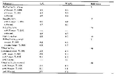 |
Table II Energy loss structure in LiNbO3 and LiTaO3 (eV)a |
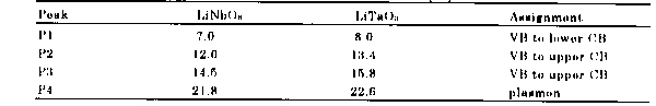 |
a The values of separation is relative to the zero loss line. VB, valence band; CB, conduction band |
| ü@ |
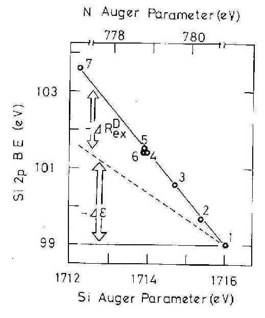 |
| Figure 1 The Si 2p Eb versus the Si or N Auger parameter (N Auger parameter is used for non-stoichiometric SiNx). 1:Si, 2:SiN0.3, 3:SiN0.9, 4:SiN1.3, 5:SiN1.3, 6:SiN1.3, 7:SiO2. [ref.6] Measured Si Auger parameters of 1, 5 and 7 are in good agreement with those by Wagner.11 |
| ü@ |
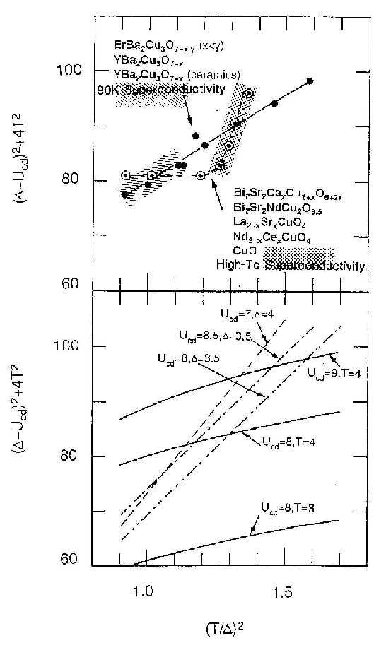 |
| Figure 2 The separation and intensity ratio of main to satellite peaks. In the upper panel the experimental relations are plotted. Proper superconductivity for each system was realized in the shaded regions. [ref.7] |
| ü@ |
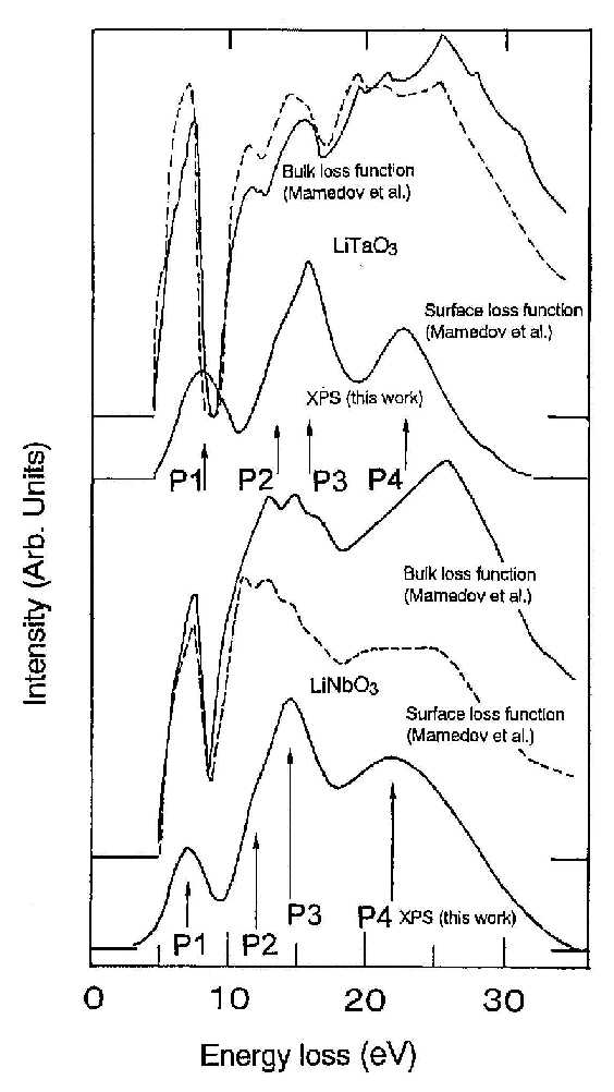 |
| Figure 3 Electron energy structures of LiNbO3 and LiTaO3 by XPS. Surface and bulk loss functions for LiNbO3 and LiTaO3 calculated by Mamedov et al.40 are also reproduced for convenience in comparison. |